How to Arrange Wiring Diagrams in a Referenced Grid
Grid System for Wiring Diagrams
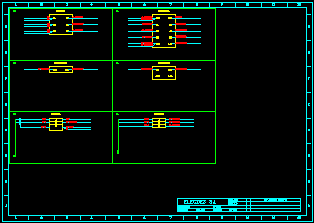
Wiring diagrams can be drawn in a referenced grid layout. Each device or terminal strip is surrounded by a grid box. Connections between devices and terminal strips are labelled by grid reference rather than component name.

The grid reference on each conductor is formatted as follows:
< grid reference > - < terminal > < conductor name >
For example: "B0-14(000141)".
The grid reference is "B0", the terminal is "14" and the conductor is "(000141)".
The rows of the grid are labelled with the letter of the grid reference, "B" in the example. The columns of the grid are labelled by the digit of the grid reference, "0" in the example.
Procedure
-
Open to the Wiring Diagram Preferences dialog of the Wiring Diagram Generator.
-
Switch to the Grid System tab, then tick the Enable / Use Grid System checkbox.
Other annotation options will be changed to suit the annotation required for conductors on wiring diagrams in a grid layout.
-
The resolution of the grid is specified by the Row and Column spacing set in the Device Spacing group, which is on the left of the General tab in the Wiring Diagram Preferences dialog.
This is the same row and column spacing used to arrange a selection of multiple diagrams.
-
Return to the Main dialog of the Wiring Diagram Generator.
-
Select only the devices and terminal strips that you want to draw.
-
Click the [Create Wiring Diagram] button at the bottom of the Main dialog of the Wiring Diagram Generator.
-
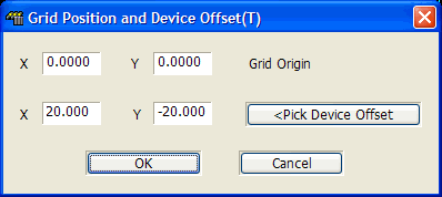
You then have the opportunity to change the location of the grid and wiring diagrams.
The grid origin and device offset in the pop-up dialog are the same origin and offset you can set in the preferences dialog shown above.
Both the origin of the grid and the offset for each device within the grid must be specified. All values should be set in drawing units.
-
For the Grid Origin, specify the top left corner of the grid.
-
For the Device Offset, specify the horizontal and vertical distance to be used between the top left corner of each grid box and the top left corner the wiring diagram contained in that box.
You can use the [ <Pick Device Offset ] button to pick this offset. This is identical to choosing the location of a normal array of wiring diagrams.
-
-
Click the [OK] button to accept the location. The wiring diagrams will be drawn at the specified location.
-
If you have chosen Individually Placed for device positioning in the General tab of the Wiring Diagram Preferences dialog then the pop-up dialog asking for origin and offset will be displayed for each diagram to be placed. You can use the [ <Pick Device Offset ] to pick the position of each diagram individually.
If the wiring diagram for a device is larger than one grid box, the box will automatically be increased in size to accommodate the device.
Using an Arbitrary Reference for Labelling Connections
Connections between devices and terminal strips can be labelled by a user entered reference called a TAGALIAS rather than using the component name. See Using an Arbitrary Reference for Labelling Connections.